Odisha kicks off India’s 1st 3D chip packaging plant
The project is being implemented by the US-based 3D Glass Solutions Inc through its wholly owned Indian subsidiary Heterogeneous Integration Packaging Solutions Pvt Ltd.
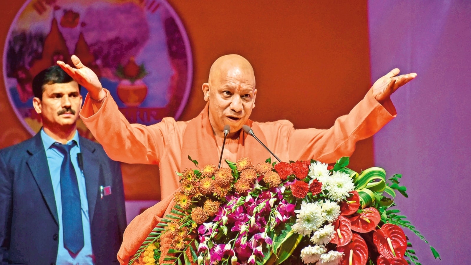
Odisha CM Mohan Charan Majhi and Union IT Minister Ashwini Vaishnaw laid the foundation stone for India’s first advanced 3D chip packaging unit in Bhubaneswar, in a big boost to India’s growing semiconductor ambitions.
The project is being implemented by the US-based 3D Glass Solutions Inc through its wholly owned Indian subsidiary Heterogeneous Integration Packaging Solutions Pvt Ltd. It is funded by Intel, among others. Intel’s CEO Lip-Bu Tan joined the ceremony virtually.
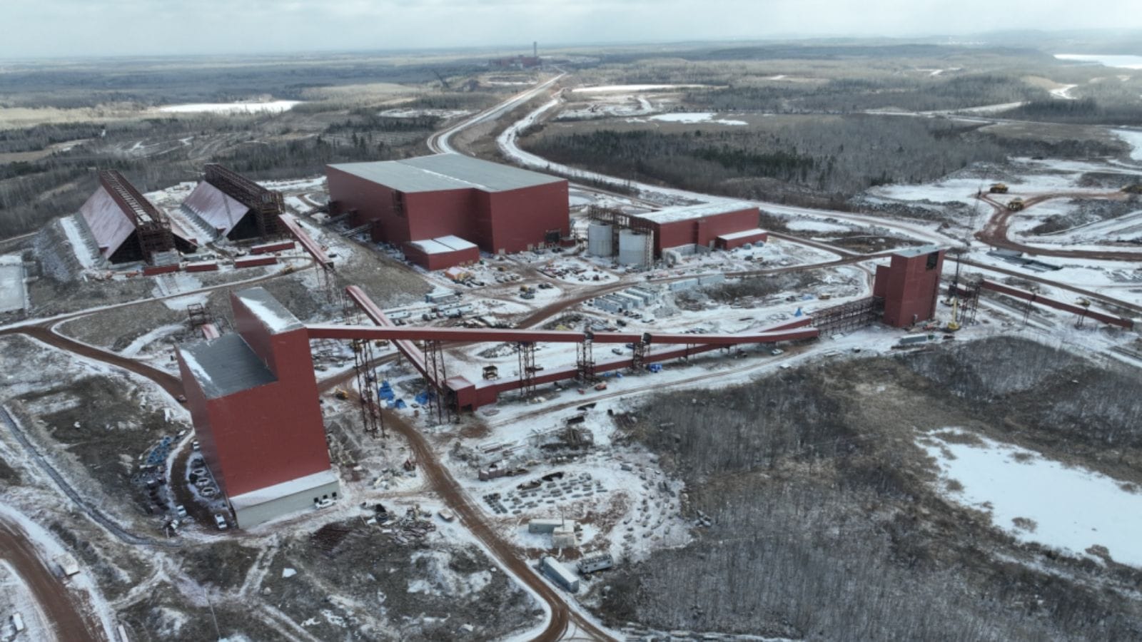
Majhi said the unit, whose Rs 1,934 crore proposal had received approval under the India Semiconductor Mission (ISM) last year, is expected to produce 70,000 glass panels annually, along with 50 million assembled units. It is among the two plants in the state that had received approval under the ISM and around 13,000 advanced 3DHI modules, Majhi said. The project will generate around 2,500 direct and indirect jobs.
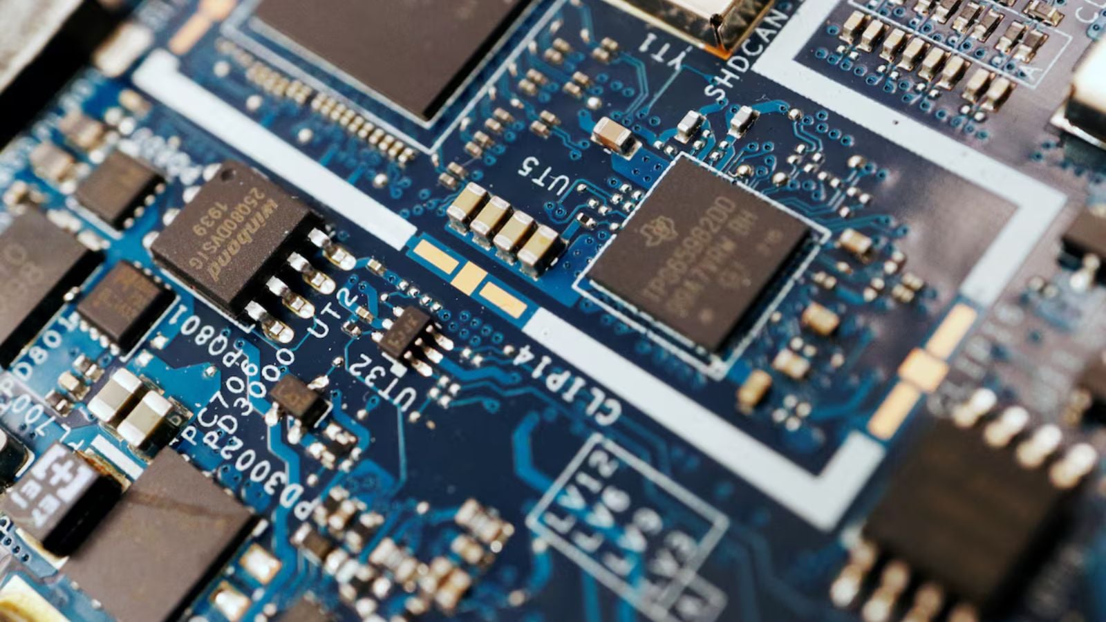
3D glass semiconductor technology is an advanced chip process that utilises specialised glass substrates to enable high-performance, three-dimensional integration of electrical components. Unlike traditional silicon, glass offers superior radio frequency performance, lower electrical loss, and enhanced thermal stability for passive component integration. The plant will assemble and package these chips.
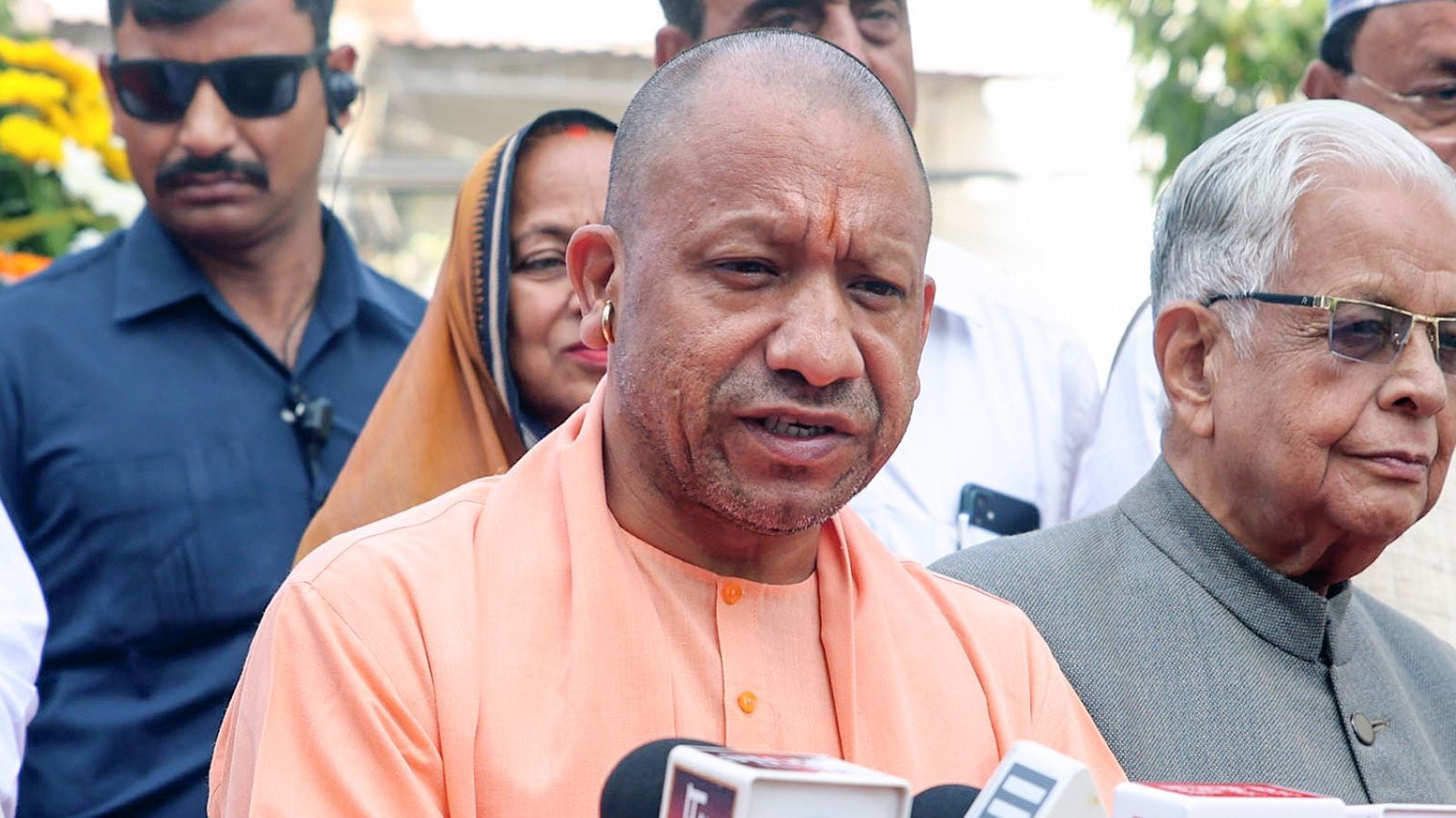
Vaishnaw called the plant’s groundbreaking a “historic” day for Odisha, adding that it marked a shift away from the usual industries that it has been associated with. “It’s very important for Odisha to have a world-class, latest technology industry here. Odisha is now becoming an IT hub (and) an electronics manufacturing hub. For years, industries like mining, metal and power have existed in the state, but now it is taking steps towards the high-tech industry.”
(The reporter was in Bhubaneswar at the invite of the Ministry of Electronics and IT)
Odisha CM Mohan Charan Majhi and Union IT Minister Ashwini Vaishnaw laid the foundation stone for India’s first advanced 3D chip packaging unit in Bhubaneswar, in a big boost to India’s growing semiconductor ambitions.
The project is being implemented by the US-based 3D Glass Solutions Inc through its wholly owned Indian subsidiary Heterogeneous Integration Packaging Solutions Pvt Ltd. It is funded by Intel, among others. Intel’s CEO Lip-Bu Tan joined the ceremony virtually.
Majhi said the unit, whose Rs 1,934 crore proposal had received approval under the India Semiconductor Mission (ISM) last year, is expected to produce 70,000 glass panels annually, along with 50 million assembled units. It is among the two plants in the state that had received approval under the ISM and around 13,000 advanced 3DHI modules, Majhi said. The project will generate around 2,500 direct and indirect jobs.
3D glass semiconductor technology is an advanced chip process that utilises specialised glass substrates to enable high-performance, three-dimensional integration of electrical components. Unlike traditional silicon, glass offers superior radio frequency performance, lower electrical loss, and enhanced thermal stability for passive component integration. The plant will assemble and package these chips.
Vaishnaw called the plant’s groundbreaking a “historic” day for Odisha, adding that it marked a shift away from the usual industries that it has been associated with. “It’s very important for Odisha to have a world-class, latest technology industry here. Odisha is now becoming an IT hub (and) an electronics manufacturing hub. For years, industries like mining, metal and power have existed in the state, but now it is taking steps towards the high-tech industry.”
(The reporter was in Bhubaneswar at the invite of the Ministry of Electronics and IT)